
Seeing the UnSeen (Archive)
Originally posted March 11, 2018.

Maria Viitaniemi is a graduate student in Physics who studies atom-scale defects in materials, because by understanding them better she can use these defects to our advantage. Her most recent project uses lasers to control electrons bound to a defect with the hope that these electrons can be used to build a quantum computer.
see (verb) \ ˈsē \ [1]
1 To perceive by the eye
2 To form a mental picture of
3 To come to know
Seeing is believing. [2] This is an idea that I struggle with when trying to communicate my research, because the things that I study are often too small to see directly. I use graphs and equations to understand what goes on in my samples, but for someone who hasn’t been studying these concepts for a long time, understanding this isn’t easy. However, in this post I will try to transform these initially confusing, unseen numbers into something beautiful.
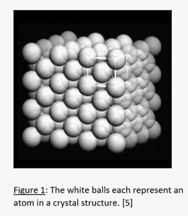
Let’s start with the building blocks of everything. These building blocks are called atoms. They are so small that 100,000 of them can fit across the width of a human hair and individuals are practically invisible to microscopes [3]. Material scientists can stack these atoms into 3-dimensional patterns called crystals (Fig. 1).
But, how do we know what these atom patterns are if we can’t see atoms with a microscope?
Building on a huge body of knowledge, Max von Laue and Lawrence Bragg developed the technique of x-ray crystallography in 1912 [4]. X-ray crystallography involves shooting x-rays at crystals, then looking at how they bounce off atoms. Because atoms are arranged in particular patterns, they will bounce off in predictable ways. Therefore, scientists were able to start drawing pictures like in Fig. 1 from pictures in Fig. 2!

Using an understanding of how crystals are structured, scientists have also discovered “mistakes” that often occur in crystal patterns. These mistakes in crystals are called defects. There are many types of defects, but my favorite is the stacking fault. To understand what a stacking fault is, let’s take a look at Fig. 3. The crystal grows from the bottom up and each layer gets stacked on top in a pattern. A stacking fault occurs when these layers are stacked incorrectly like in Fig. 4. A stacking fault is a flat 2-dimensional sheet in a 3-dimensional crystal.

This stacking fault is the stage for a show full of dynamics. When I shine a laser on a stacking fault, particles called electrons get excited. When they get excited, electrons leave their place in the crystal and start to move around on the stacking fault. Additionally, when they leave their place, electrons leave behind a “hole”. Holes act like bubbles and can also move around. With each laser pulse, thousands of electrons are excited and holes are created. They move around the 2 dimensional stacking fault, but they can’t run around just anywhere in this sheet. To know understand where they will go, we must take a look at the “landscape” of a stacking fault.
If stacking faults are flat, how can they have an interesting landscape? Aren’t they equally likely to go anywhere?
In terms of physical shape, yes. Stacking faults are mostly flat; however, their potential energy landscape usually isn’t flat. Potential energy is an object’s energy based on its position or configuration. For example, when I stand on a chair, I have increased my potential energy due to gravity; I can release this stored energy by jumping off the table. For another example, when I squeeze a spring, I have increased the springs potential energy; this can be released when I shoot the spring at my friend. An object’s potential energy landscape is a representation of how much potential energy that object would have at any point in that space. The more potential energy an object would have at a position the higher its potential energy landscape. So if I climb onto an even higher stool or squeeze the spring harder, my potential energy landscape will be higher. Similarly, different things the electron or hole’s environment can increase or decrease it’s potential energy landscape. And just like a ball wants to roll to the bottom of a hill, the electrons and holes want to go to a place with the lowest potential energy. In this way, the potential energy gives us a new way to visualize the environment of the electrons and holes and help us understand how they will move.

Figure 5: An example of a potential energy landscape. [7]
Good imagination. But how do you know this is what’s going on if you can’t see electrons or holes?
Even though we can’t directly see electrons or holes, we can see it when the electron and hole come back together (remember that a hole was just the bubble left behind when an electron got excited). When an electron and hole recombine, they release the energy that was used to separate them. This extra energy is released in the form of light. In my lab, we collect this light using a microscope. By seeing where the most light is released, we know where the most electrons and holes are. We can also see how long it takes for the electrons and holes to find each other by looking at when the light is released. We might not have high enough resolution to see individual electrons, but we can build a picture of what individuals are doing by looking at the light released by large populations.
This concludes a brief description of my research and I hope that it has given you a taste of how scientists can see using graphs and experiments. I also hope that you take a moment to marvel at the imagination and resourcefulness of the scientists who first came up with these beautiful images of crystals and potential energy landscapes, especially considering about how much more complicated they could have made these ideas.
[1] A portion of the definition from, https://www.merriam-webster.com/dictionary/see
[2] 1637, https://idioms.thefreedictionary.com/seeing+is+believing
[3] Here I am referencing optical microscopes which were the most accessible at the time of development of crystallography. Electron microscopes have been able to image atoms.
[4] https://learn.crystallography.org.uk/learn-crystallography/history/, https://en.wikipedia.org/wiki/X-ray_crystallography
[5] Image from https://www.nde-ed.org/EducationResources/CommunityCollege/Materials/Structure/metallic_structures.htm
[6] Image from http://www.microscopy.ethz.ch/TEM_ED_examples.htm